MAKE A MEME
View Large Image

| View Original: | Nanoscale Blasting Adjusts Resistance in Magnetic Sensors (5941045222).jpg (742x1037) | |||
| Download: | Original | Medium | Small | Thumb |
| Courtesy of: | commons.wikimedia.org | More Like This | ||
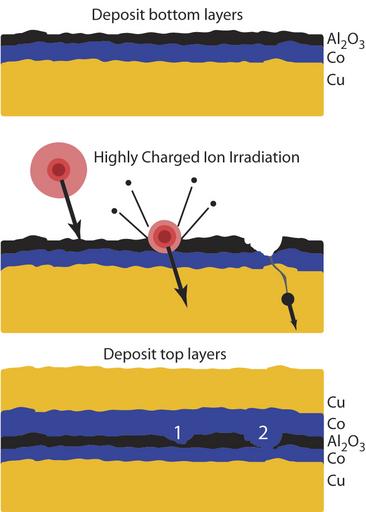
| Keywords: Nanoscale Blasting Adjusts Resistance in Magnetic Sensors (5941045222).jpg Cartoon illustrates new NIST technique for selectively modifying resistance of a semiconductor device layer Top First layer - in this case a composite of copper and cobalt - and an insulating buffer layer of aluminum oxide is deposited Buffer is about one nanometer thick Middle Highly charged xenon +44 ions strike the buffer layer digging nanoscale pits Bottom Top conducting layer of cobalt and copper is deposited Pits reduce the electrical resistance of the layers and may function as nanoscale GMR sensors embedded in a MTJ sensor Credit NIST Disclaimer Any mention of commercial products within NIST web pages is for information only; it does not imply recommendation or endorsement by NIST Use of NIST Information These World Wide Web pages are provided as a public service by the National Institute of Standards and Technology NIST With the exception of material marked as copyrighted information presented on these pages is considered public information and may be distributed or copied Use of appropriate byline/photo/image credits is requested https //www flickr com/photos/usnistgov/5941045222/ Nanoscale Blasting Adjusts Resistance in Magnetic Sensors 2007-08-16 12 24 https //www flickr com/people/63059536 N06 National Institute of Standards and Technology PD-USGov National Institute of Standards and Technology https //flickr com/photos/63059536 N06/5941045222 2016-09-07 02 35 56 United States Government Work Uncategorized 2016 November 30 | ||||