MAKE A MEME
View Large Image

| View Original: | Advanced Measurement Laboratory; Nanofabrication Facility; Chip Ovens (5884870010).jpg (300x201) | |||
| Download: | Original | Medium | Small | Thumb |
| Courtesy of: | commons.wikimedia.org | More Like This | ||
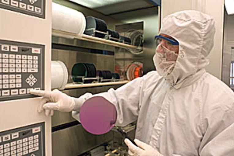
| Keywords: Advanced Measurement Laboratory; Nanofabrication Facility; Chip Ovens (5884870010).jpg Russell Hajdaj prepares silicon wafers that will be baked as part of the processing required for producing new types of semiconductor devices Copyright Robert Rathe This image may be used for any NIST purpose Correct photo credit must be provided Other organizations may use this image without charge for editorial articles that mention NIST in accompanying text or a caption Correct photo credit must be provided Stock art use requires permission and may require payment to the photographer To receive a high resolution version send an email with the image AV number 06CNST003 and title to inquiries nist gov Disclaimer Any mention of commercial products within NIST web pages is for information only; it does not imply recommendation or endorsement by NIST Use of NIST Information These World Wide Web pages are provided as a public service by the National Institute of Standards and Technology NIST With the exception of material marked as copyrighted information presented on these pages is considered public information and may be distributed or copied Use of appropriate byline/photo/image credits is requested https //www flickr com/photos/usnistgov/5884870010/ Advanced Measurement Laboratory; Nanofabrication Facility; Chip Ovens 2011-06-29 08 33 https //www flickr com/people/63059536 N06 National Institute of Standards and Technology PD-USGov National Institute of Standards and Technology https //flickr com/photos/63059536 N06/5884870010 2016-09-07 02 52 16 United States Government Work Uncategorized 2016 December 20 | ||||